Kicad: Creating schematic components and libraries
I’ve had some trouble piecing together how to deal with custom schematic components in my PCB design package of choice, Kicad. It took too much searching and trial and error to get to grips with the process, so I’ve decided to write my own detailed article about it. This guide applies as of version 4.0.4-stable. I’m using the Windows build.
Please do note, this article will only cover schematic components; I will not touch on the actual PCB footprints here. In Kicad, the two are very distinct; they are only connected when you finish designing your schematic, and you assign footprints to each of the components in it.
Library structure
In Kicad, all files are essentially plain text files, meaning you could edit them with a simple text editor like Notepad or TextEdit. A library (.lbr) file is one such plain text file, in which a series of schematic components are defined by name, a set of pins, and a drawing. In addition, there is a .dcm file for every library file, which contains any documentation and description for the components contained within the library.
Kicad comes with a set of libraries of its own, which are typically stored in a read-only location. As a result, if you want to customize or create new components, they should be saved in a library within your documents, or your project directory. You can choose to maintain your own main set of libraries that all your kicad projects can access, or you can save libraries in project folders, making them local to just that project.
The location you save your libraries is a matter of personal preference, so don’t dwell on it too much.
Creating an entirely new component from scratch
Before diving in, I also cover how to create a component based on an existing one. Skip ahead to Creating a modified copy of an existing component if that’s what you’re after.
For the purposes of this guide, I’m starting the with the assumption that you don’t have an existing library file to save to. If you do, you may skip a few steps here and there.
First, open up Kicad, and create or open a project if you haven’t already.
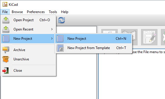
In the right side of the main window, click the “Schematic library editor” button, 2nd from the left.
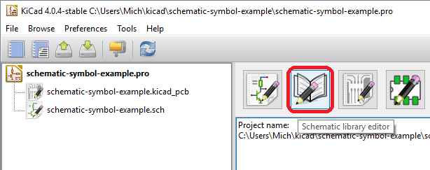
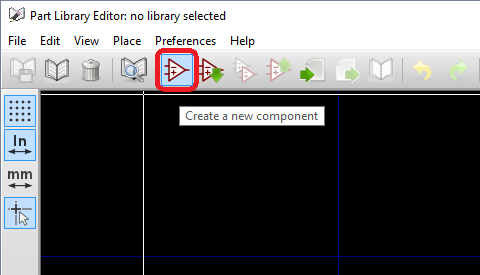
This launches Kicad’s “Part Library Editor”, which is part of “Eeschema”, the schematic editor. To create a new component, click the “Create a new component” button in the toolbar.
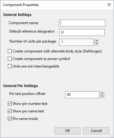
In the “Component Properties” dialog that shows up, enter a name for your component.
You can also change the “reference designator”; this is the letter that is followed by a number, and is shown by the component in schematics. For resistors, this is usually “R”, for capacitors “C”, and so on. Usually you’ll be making a component for a chip, in which case the default “U” should do fine.
The other options in this dialog are fine in most cases, and I won’t cover them here. Of course, feel free to experiment. You can access most of these options later by clicking “Edit component properties” in the toolbar.
Click OK when done.
You should now be looking at the following screen:
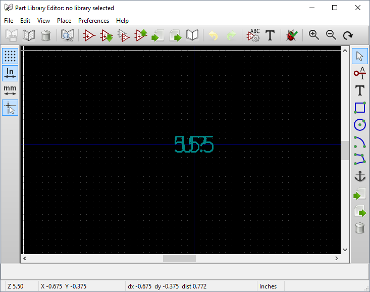
The blue cross through the middle indicates the centre of the new schematic component. Eeschema has also dumped both the component name and its designator right in the centre, over the top of each other.
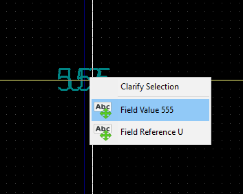
Let’s move that text out of the way. Move your mouse over the text and press “M” (move) on the keyboard. Since there are multiple items near/under the cursor, the program will ask for clarification; what exactly is it that you want to move? This flow is common throughout Kicad.
In the context menu shown, click “Field Value”. You can move your mouse and the name will follow it. Click again where you want to position it. I recommend moving it up from the centre. Repeat the same for the designator (“Field Reference”) afterward, moving that one down. For this one, you won’t need to clarify your selection.
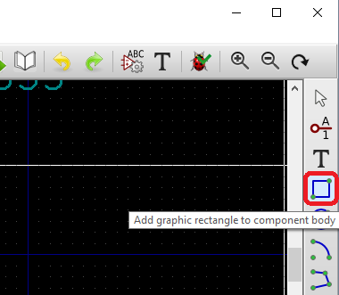
Next up, we’ll draw an outline. For most integrated circuits (ICs), a rectangle will do. In the toolbar on the right, click the “Add graphic rectangle” button.
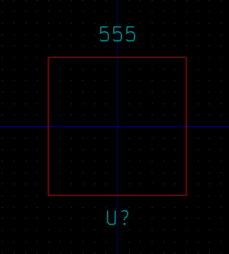
Now start drawing the rectangle by clicking once where you want the top left corner to be, then clicking again where you want the bottom right one. Try centring it neatly around the blue cross. You should end up with something like this:
If you need to move the rectangle after you’ve finished drawing it, you can do so by placing your mouse over one of the edges and pressing “M” (move) on the keyboard. This will pick up the entire rectangle and release it where you click next.
If you want to move just one of the edges (resizing the rectangle), place your mouse over the edge, and press “G” (grab) on the keyboard. This will pick up just that edge and let you resize the rectangle in the direction of that edge. Click again when the edge is where you want it.
Grid alignment for pins
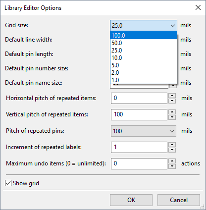
Next up, we’ll add the component’s pins to the schematic symbol. Before that though, it’s important to point out the grid. Eeschema’s schematic editor grid, by default, is set to 0.100 inches (also written as 100 mils). However, the grid of the component editor defaults to 0.025" or 25 mils. This increased precision is helpful for drawing more detailed shapes, but it’s easy to trip up with pin placement because of it.
IMPORTANT: When placing pins, always ensure that the connection point of the pin is placed on a multiple of 0.1" or 100 mils from the centre point. When set to a grid of 0.025" or 25 mils, that means you need to count 4 grid dots per pin. If you don’t feel like having to count, it’s easier to change your grid size when you’re about to place the pins.
You can change the grid size in Preferences > Component Editor Options > Grid size and set it to 100.0 mils for working on pins. Don’t forget to change it back if you need to work on more detailed drawing.
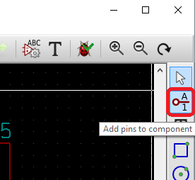
We’ll first add the power pins for our 555 component; VCC and GND. Click the “Add pins” button in the right toolbar.
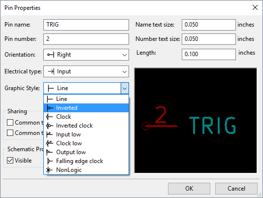
With that tool selected, click where you want your first pin. For the VCC pin, it’s customary to place it above the rectangle. Having clicked, the “Pin Properties” dialog window shows up:
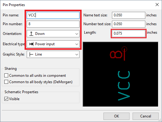
There are a few fields to pay attention to here:
- Pin name: This describes the function of this particular pin. Usually a short abbreviation. Use the naming used in the datasheet here, to minimize confusion.
- Pin number: Perhaps the most important field, this is the pin number as shown on the datasheet. This will be important when mapping to a footprint, so be sure to get this right.
- Orientation: the direction in which the line for the pin is drown. Not very important as it can easily be rotated later, if needed.
- Electrical type: This is used when running the Electric rules check (ERC) in the schematic editor later. It determines what kind of pins from other components may be connected to this one. In this case, “Power input” means we need to connect something that acts as a power output to it.
- Length: Length of the line drawn leading to the connection point. Set this to taste to work with the rest of your symbol.
Hit “OK” when you’re happy with your values. You now have the opportunity to move the pin again, as it moves around with the mouse cursor. If at this point you notice you got the orientation of the pin wrong, it can be corrected by pressing the “R” (Rotate) key on your keyboard until it is corrected. Click where you want your pin to end up to finish placing it.
Note: you can always bring the “Pin Properties” dialog back for an existing pin by moving your mouse over the pin and pressing the “E” (Edit) key on your keyboard.
Repeat this for each of the pins. GND is also a power input. For the 555, all other pins are inputs, except the “out” pin, which, as you might expect, is an output.
For our example component, the 555, there are a couple of special cases in the “Trig” and “Reset” pins. These are both inverted, meaning that they function with the opposite input signal than your might expect. For this we use the “Inverted” graphic style. There are several more built-in styles you can choose from here. It’s best to have a look at this list before manually drawing shapes by your pins.
After setting up all your pins this way, you should end up with something like the following:
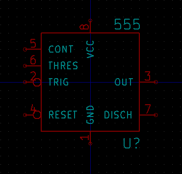
The symbol with all its pins is now finished. We’re not entirely done yet, though. To make a well-rounded symbol, we should add some more information.
The name of the component was already set from the beginning. If it needs changing, place your mouse over the name, and press “E” (Edit) to bring up the “Component Name” dialog. You can change the name there, and if you wish, change a variety of options regarding how the name is displayed.
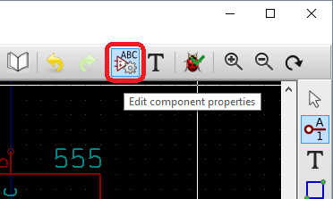
To add further information, click the “Edit component properties” button in the top toolbar.
The “Options” tab isn’t particular interesting, so let’s head to the “Description” tab. Here you can describe the function of the component. I tend to go with the first line in the datasheet. For the 555 this is “Precision timer”.
You can also add a set of keywords that might help in finding the component if you don’t remember the exact name. Further, you can add the URL to the datasheet, or refer to one saved on your computer.
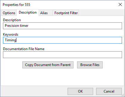
Under the “Alias” tab you can add any alternative names for this component.
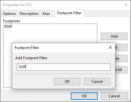
Finally, in the “Footprint Filter” tab, you can add the names of any footprints this component is manufactured in. This makes it easier to filter to relevant footprints when making footprint assignments after completing a schematic diagram. The datasheet will usually list all available footprints for the device. For the 555 timer, these are “DIP” and “SOP”.
To add a footprint filter, click the “Add” button, write the name of the footprint in the dialog that shows up, and click “OK”.
Click “OK” when you’ve finished editing your component’s properties.
Saving to a new library
Now, since we don’t have a library yet, let’s create a new one starting with the component we’ve just put together. In the top toolbar, click the “Save current component to new library” button.
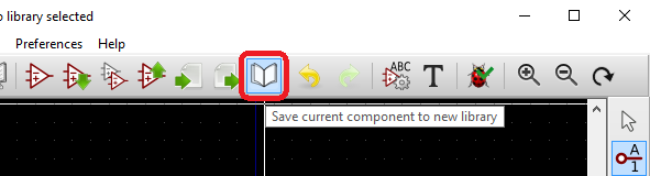
Navigate to a folder where you’d like to save your new library, and make sure to give it a descriptive file name. The file name, minus the “.lbr” extension will be used when a list of available libraries is displayed. Click “OK” when you’re happy with the location and name.
Adding a library to Eeschema
Kicad now shows a helpful message informing us that this new library will not automagically show up, ready to use. We’ll need to tell Eeschema where to find it, before it can be used in the editor at all.
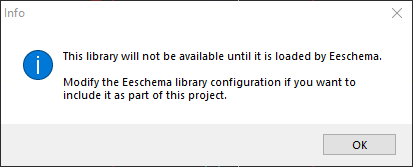
And indeed, notice how in the title bar of the schematic component editor, it still reads “no library selected”. This is a little confusing, since we just saved a new library. Personally, I expected that that would automatically become the selected library.
It turns out that only libraries Eeschema has been specifically made aware of can be a selected library in the schematic component editor. You could click “Select component library”, but the newly saved library would not be listed there.
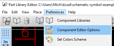
So, let’s correct that situation. Open up “Preferences > Component Libraries” in the menu bar.
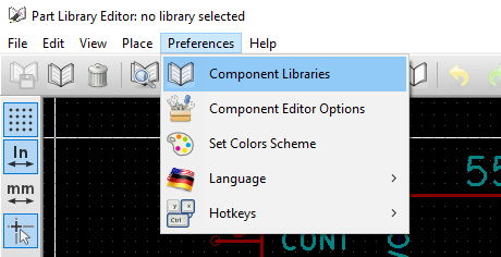
In the window that shows up, the currently available libraries are listed. Click the “Add” button on the right to find your library file; select it and hit OK.
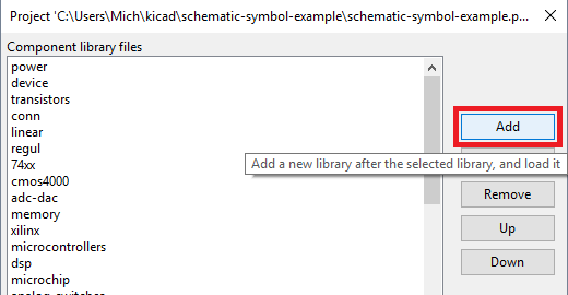
After doing that, your library should have been added to the list; you may need to scroll to see it. Click “OK” to close the window. Your library will now be available to both the schematic component editor and the regular schematic editor, as they are both part of Eeschema.
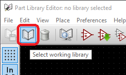
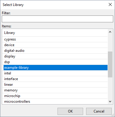
Now you can click the “Select working library” button in the top toolbar, and then pick out the library we just made available; click “OK” to confirm.
Making changes after saving to a library
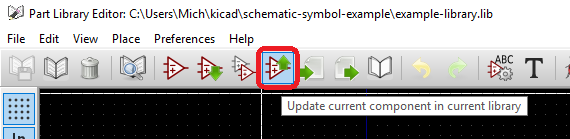
If you wish to make any more changes to your component now, go ahead. You can then update the component within the selected library, by clicking the button aptly named “Update current component in current library” in the top toolbar.
Note: this button is a bit strange, in that it doesn’t save the library file to disk, but it ensures that the component on your screen is part of the working library in memory. This operation becomes particularly important / useful when copying or modifying components from one library to another, but more on that later.
A secondary note on “Update […] in current library”: If you have changed the name of the component after adding the component to a library, pressing this button will create a new component, with the new name in the select library, alongside the one with the old name. As far as I know, there is no straightforward way to remove it from the library, other than carefully editing the .lbr file with a text editor. If you want to poke around with that, please be sure to either use version control, or make a copy of the intact file first, in case you mess something up.
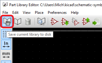
To actually save your library to disk, hit the “Save current library to disk” button. You could skip the step before pressing the “Save current lib…” button, and Kicad will offer you the choice of including any changes you’ve made to the component you’re looking at, so long as it was already part of that working library.
You’re done!
That’s it, you’ve created a new component from scratch and created a library for it, and then made that library available for Eeschema to use. You should now be able to get started in your schematic with the new component.
Creating a modified copy of an existing component
In many cases, the schematic component you need is only slightly different from one that’s available in the standard libraries. For instance, if you’re using an analog-to-digital (ADC) converter IC that isn’t available, it’s useful to start from an existing ADC in the library, and tweak things as needed.
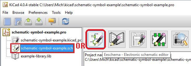
Open up your schematic by double clicking the .sch file in Kicad’s main window. Alternatively, you can click the “Eeschema” button on the right, it’s the first one from the left.
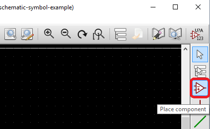
Start out by finding a base component in Eeschema, while taking note of the library it’s in. Press “A” (Add) on the keyboard, or click the “Place Component” button in the right toolbar (3rd one from the top). Then click anywhere in the working area to bring up the “Choose Component” dialog.
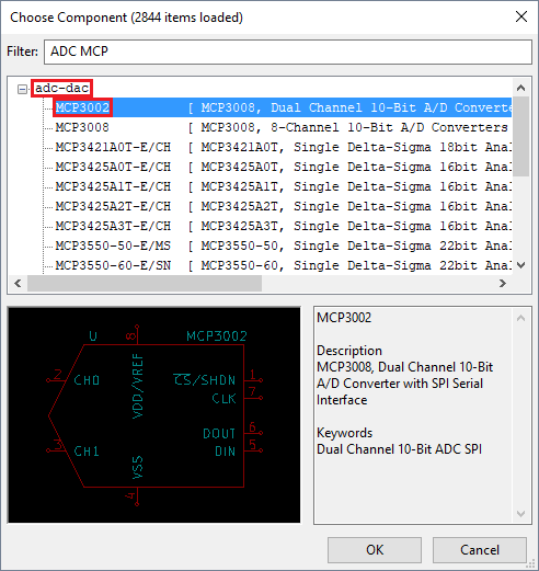
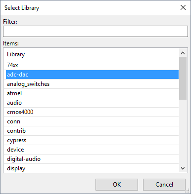
I want to create a schematic component for Microchip’s 3202 Analog to digital converter, but it appears Kicad only has one for the MCP3002. It’s a good one to base it on. Take note of the library name, here “adc-dac”, and the component name, here “MCP3002”. Click “Cancel” or press “ESC” on the keyboard to close the dialog without selecting a component.
You can now close Eeschema if you wish.
Open up the “Schematic library editor” again from Kicad’s main window.
Now, we want to load up the existing component in the editor. We start by selecting the containing library as the working library. Click the “Select working library” button in the top toolbar (2nd from the left).
Look for the library containing your component and select it, confirming with the “OK” button or the enter key.
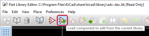
In the title bar, you will now see the path to the selected working library, possibly along with “[Read Only]”. No component is shown yet, though. To pick the component we want to work from, click the “Load component” button in the top toolbar.
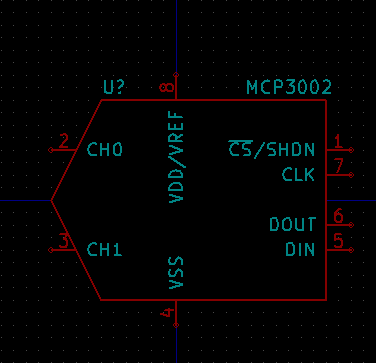
This brings up the same “Choose component” window as we saw in the schematic editor, except now only components from the working library are shown. Searching for “MCP” brings up the MCP3002 I wanted to work from. After selecting the component you want, click “OK” to load this component in the editor.
Now you can make any edits you need to this schematic component. For me, all that needs to change is the name, as the rest of the MCP3202 layout (pin numbers and function) is identical to the MCP3002. To change the name, as seen earlier in the article, place your mouse over the name text (MCP3002) in this case and press “E” (Edit) on the keyboard. Change the name and click “OK”.
For more details on the edits you can make, refer to the above section on making an entirely new component.
After you’re satisfied with the changes you’ve made, you can save the component to a new library, or an existing library. The steps involved ar a bit different.
Saving a component to a new library
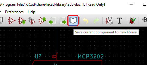
Similar to creating an all-new component, to save the component you modified to a new library, click the “Save to new library” button in the top toolbar.
Find a good location for the new library and save it. Kicad will then show a notice about the library not being available until you load it in Eeschema. Have a look at Adding a library to Eeschema above to sort that out.
Once that is sorted, you’re done; you can now go back to the schematic editor, and find your slightly altered component with a new name in your newly created library.
Saving a component to an existing library
To save to an existing library, we need to change the working library. Click the “Select working library” button in the top toolbar again, and find the existing library you want to add this component to. If your existing library is not listed here, but you have the .lbr file somewhere, follow the steps in Adding a library to Eeschema to sort that out, then return to “Select working library”.
Select your library and click “OK”. Now click the “Update current component” button to add the component to the working library.
At this point, the working library has changed in memory, but you’ll also need to click “Save current library” to commit those changes to the actual library file.
The schematic component is now available in your existing library. You can go back to the schematic editor, and find your slightly altered component with a new name in your existing custom library.
Well, that about wraps it up. I hope this article removes any confusion on how to go about making a new schematic component, or starting from an existing one.